News
2026-02-12

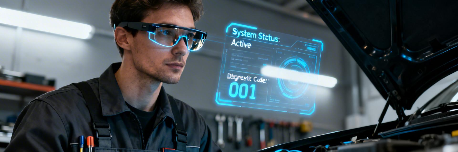
Recent benchmarks for wearable electronics show design teams commonly aim for 30–60% area reduction and 20–40% weight reduction. For users, this means shifting from bulky "gadgets" to lightweight, all-day wearable AI glasses. This guide translates technical targets into actionable decisions for US-focused engineering teams.

Ergonomics dictate temple envelopes often limited to 6–12 mm (0.25–0.5 in). By shaving PCB area, we allow for 30–40% larger batteries within the same frame volume, directly solving the #1 user complaint: short battery life.
| Metric | Engineering Target | User Impact |
|---|---|---|
| Area reduction | 30–60% | Sleek, fashionable frame designs |
| Weight Budget | 8–18g per side | Reduces nose-bridge fatigue/slippage |
Antennas need 5–8 mm clear zones to function; heat-producing ICs should have direct thermal vias to internal copper. Placing heavy modules like the PMIC in the temple maintains balance.
| Zone | Preferred items |
|---|---|
| Temple | Battery, PMIC, SoC |
| Bridge | IMU, Microphones |
Hand-drawn diagram, not an exact schematic
| Feature | Standard Wearable | AI Glasses (Optimized) | Advantage |
|---|---|---|---|
| Via Tech | Through-hole | Stacked Microvias (ELIC) | 40% Higher Routing Density |
| Trace Width | 5-6 mil | 3-4 mil | Ultra-compact Footprint |
| Flexibility | Rigid + Connectors | Seamless Rigid-Flex | Better Durability in Hinge |
Miniaturized designs often use HDI with 6–8 layers. While HDI increases per-board cost, it drastically reduces enclosure size and assembly complexity for dense BGAs. Prioritize wafer-level CSPs (WLCSP) to minimize Z-height.
Design PDN with distributed decoupling. Use thermal vias under hot ICs to spread heat into internal copper planes or hinge structures. This prevents localized "hot spots" that could be uncomfortable for the user's temple.
| Rule | Default |
|---|---|
| Diff pair tolerance | ±5–10 mil |
| Capacitor Placement | 2–4 mm from pins |
John Smith, Senior FAE & Hardware Architect
"When routing for AI glasses, the biggest pitfall is ignoring the hinge's mechanical stress on the flex layers. I always recommend a 'tear-drop' pad design for all microvias on the flex portion. Also, avoid placing any components within 3mm of the actual bend line to prevent solder joint cracking during thousands of temple fold cycles."
Q: What is a safe minimum bend radius for rigid-flex in AI glasses?
A: Target a dynamic bend radius at least 10x the flex stack thickness. For ultra-thin flex (≤0.15 mm), 1.5–2 mm is common.
Q: How do microvias affect cost?
A: HDI increases per-board costs but enables 40%+ more components in the same space, often reducing the total number of boards needed.
Q: Which tests are most critical?
A: PDN stability, hinge bend-cycle durability, and thermal skin-contact safety are the top priorities before pilot production.